"I grow cold… I grow cold… I shall stoke the bottom of my firebox old". With apologies to T.S.Eliot and his poem "The Love Song Of J.Alfred.Prufrock".
This is the fifth article in a series which describes the way I have built a train set which can be completely controlled from a computer. In the first articles, I discussed some of the computer control options and issues needing consideration in a circuit design. In the third and fourth, I presented the circuit and described its electrical operation. In this article, we will look at the construction of the circuits and I'll describe some good all purpose tips to help you on your way.
When I started in the electronics hobby, I was young and keen to learn but short on confidence. It was good to find simple circuits for interesting designs but it was even better to be able to purchase a kit because it simplified the construction task and reduced the chances of wiring error. In time, I learned a great deal about circuit design and debugging, discovered how much more there was still to learn and I decided to start modifying published designs to "add features" or do completely different things. Only then did I discover the flexibility, joy and advantages of "scratch building".
It is normal that published circuit designs are accompanied by a custom designed Printed Circuit Board. When constructing a project using a pre-designed PCB, the tricky work of optimising the component layout and the under-board wiring are essentially done for you in advance. This project includes a rough component layout suggestion but the fine details and the construction method are left up to each reader. On the one hand, this allows everybody the opportunity to become more "intimate with the circuit" and on the other, it makes construction of the circuit a little more challenging!
Because construction of the train controller will be a little trickier than a PCB based project, I’ve tried to draw on my experiences to provide lots of tips and suggestions about the way the circuit could be built and tested using the scratch building approach. Of course, these principles can be applied equally well to any other circuit you may choose to construct and so if scratch building is something you have not previously attempted, read on, take risks, discover new ideas and enjoy! Scratch building is how the electronics hobby and profession started many years ago and there is something to be gained in immersing yourself in the craft of the scratch building experience and seeing your work come to life!
Choosing a construction technique
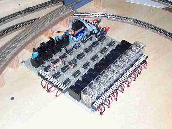
There is an abundance of different approaches which could be followed to construct a circuit such as the train controller. I constructed my circuit on matrix board (as shown in Figure 1) rather than on a custom designed Printed Circuit Board because I found this to be relatively cheap and I do not have the tools for designing and fabricating my own PCBs. The matrix board is also a good approach if it is intended to change and adapt the design along the way and in general, hobbyists who like to experiment with one off circuit design or who like to modify circuits as they progress usually prefer such a method of construction.
Figure 1 I chose to construct the train controller circuit on a piece of matrix card
Matrix board is a generic name for a fibreglass or Bakelite board with a matrix of holes drilled through it. A particular type of matrix card is sold under the name "Veroboard" and is a type of single sided printed circuit card with tracks that run from one side of the card to the other linking the matrix of holes as a series of parallel lines. However, I have also used matrix boards which contain no copper, just small pads or which contain only a grid of power traces.
Regardless of the type of matrix card, components are generally mounted as they would normally be on a custom designed PCB. In the case of Veroboard style cards, because the generic copper traces are parallel and do not connect your circuit correctly by default, you must cut the copper traces in numerous places (using a knife or by twisting a small drill bit in the vacant holes) and then joining the resulting "segmented horizontal" traces together with pieces of insulated wire (generally fine wire such as wire wrap wire).
A variation of matrix board scratch building is the wire wrap approach. In the past, I have wire wrapped many different projects and have found wire wrapping to be the best approach when there are a very large number of DIL ICs in the design.
For those unfamiliar, wire wrapping is a technique where all the connections to DIL devices are made by wrapping fine wire very tightly around special IC sockets which have long, square profile posts rather than the familiar stubby socket legs. Soldering is only required when there are discrete components (such as resistors, capacitors etc). The discrete part of the circuit is built using traditional matrix board techniques and when it is too cumbersome to solder the discrete components directly to the base of the wire wrap posts, special component carriers can be used or a flying wire wrap lead may be soldered to the discrete part and wrapped to the DIL socket leg.
The down side about wire wrapping a circuit is that the IC sockets are generally a little more expensive than standard DIL sockets and the solder side of the board becomes thicker because of the protruding length of the sockets’ wire wrap posts.
At the other end of the home brew spectrum, it is of course possible to design and build a specific PCB and this would definitely simplify and speed construction if you intend to make a number of similar train controller cards. You may consider this option if you have the facilities and if you wish to control a larger train set.
Because it is always possible to optimise the routing of a custom designed PCB’s tracks to a particular circuit, matrix board and wire wrap implementations are generally slightly larger than a modern multilayer PCB. But no matter which construction method you choose, don’t fall into the trap of not allowing yourself sufficient room between ICs – particularly in the side to side dimension.
Modifying and constructing the train controller card
A quick glance at the parts list presented in the third article will reveal that this is a project which contains a relatively large number of individual components. The reason for this proliferation becomes clear when the highly parallel (or duplicated) nature of the design is recognised. Because the design is highly parallel, it easily lends itself to modification to suit the requirements of each constructor and their train set.
There are at several ways in which the basic design could be adapted.
Firstly, the replicated parts of the circuit can be further duplicated (or reduced) to adapt to the size of your particular train set and to the number of trains which a single train controller card is required to manage.
Secondly, if you feel strongly about the number of D to A steps required for realistic train operation, you could modify the programmable power supply section to increase the number of bits in the D to A converters.
Thirdly and perhaps less basically, you could choose to not implement the programmable power supplies in the circuit at all. If instead of the programmable power supplies, you use manually operated model train throttles, the computer can be used to control the switching of points and the tracking of trains as they move about the layout – but the direct operation of the throttles could remain manual as tradition holds. This is indeed an interesting proposition and if you are keen to follow this approach, you will also need to delve deeply into the example train controller software to modify it.
After you’ve settled on a circuit design, you will need to very carefully plan a physical component layout. It is always best to purchase ALL of the components first and then take a full size sheet of paper and accurately plan your component layout BEFORE you start construction. It is even a good idea to place the main components or sockets onto the matrix card (without soldering) just to play around with different layout concepts.
If you start building the circuit onto a matrix card without all the components in hand or without accurately planning the component layout, part way through the construction you will run a high risk discovering that the components will not fit onto the card in the way you first thought. Trying to recover from a layout miscalculation without removing components and reworking can be a major hobbyist’s disaster – so be very careful to keep your enthusiasm to start construction in check.
In general, the primary goal when defining a component layout is to minimise the total length of point to point wiring. The best way of achieving this goal is to divide the overall circuit into smaller logical sections and locate the components within each section as closely as possible to each other. The circuit diagrams presented in the last articles are already split into logical sections and so some of the planning work has already been performed for you!
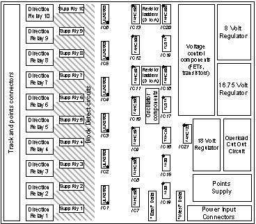
Figure 2 Suggested component layout for train controller card
Figure 2 shows the undetailed layout of components I chose for my implementations of the train controller card and reflects the replicated nature of the block circuits and the serial nature of the shift register circuits. In order to simplify the wiring of the relay driver devices (IC1 to IC6), I chose to orient these in the opposite direction to that of the other chips but you of course can choose to suit yourself.
Whilst most of the components in this circuit always appear in the same physical packaging as I have drawn, there are a tremendous variety of relay and heat sink designs on the market and it is probable that the relays and heat sinks you choose will be different from those I used. Particularly because of the relays and heat sinks, your own layout may differ slightly from that presented in Figure 2.
In order to keep the overall dimensions of the card to practical limits, I chose to closely pack the components for the block detection circuits in between and around the relays – this is also where the majority of components are to be found so the component density is high.
I mounted many of the resistors in the D to A resistor ladders in a radial way with one side of each resistor soldered under the matrix board (as per convention) but the other side soldered in mid air (flying connections) on the component side of the card. Again, it is not necessary for you to follow this practice but it does help keep the overall size of a matrix board implementation closer to that of an equivalent PCB.
As you plan your component placement on top of the card, it is just as important to think about how you will need to wire the components underneath the card. In a custom designed PCB, holes are usually drilled as close to the component body as possible so that component lead length (and component movement) is minimised. The tracks on the PCB connect components to each other by curving around other holes and tracks. In a matrix card implementation, there are no tracks or the tracks do not always go where you want them to – so another approach is required.
With matrix cards, it is far easier to orient parts with longer legs (such as resistors, capacitors and diodes) so that the long legs can be bent to be directly soldered to the other components which need to be connected. Sometimes, this means that some of the parts’ leads need to be bent into an appropriate shape on the component side of the card, and sometimes the leads poking through to the solder side need to be shaped to find other parts. In this way, the long component leads take on some of the shapes that the tracks on a custom designed PCB would have taken.
To avoid short circuits now (and far more importantly, later), you must be *meticulous* to allow plenty of space around these bent component leads and to ensure that you *never* route a bare lead over the top of or too close to any other leads or copper tracks. When you will be relying upon a bent lead to make a connection, you will sometimes need to slide a small length of insulating spaghetti onto the lead to assure insulation.
For the majority of under board connections though, it is best to avoid the temptation to bend the leads if the wire route will be more than a few millimetres. Instead, use short lengths of insulated wire. Trim the component leads close to the holes where they protrude onto the solder side and then run flying lengths of insulated wire across to the places where the parts need to be connected. In the end, using insulated wire for the majority of under board connections is the safest approach.
In a simple matrix board circuit, just about any sort of insulated wire will be fine but in a circuit which has a large number of components (and so a large number of flying connections) it is best to use the smallest diameter wire which you can get away with electrically. The more wire connections you need to make, the messier the underside of the matrix card will become and the harder it will be for you to manage both during the construction and later during any debugging which might be necessary.
Wire wrap wire is undoubtedly the most appropriate for any connection in this project other than those related to the power supplies and those carrying higher currents. If you’ve never used wire wrap wire before, it is also a good idea to invest in a cheap wire wrap wire stripper and these often come with wire wrap tools. Just because wire wrapping is more often used professionally than by hobbyists, be careful not to fall into the trap of believing that all wire wrap tools and wire are exorbitantly expensive. Hobbyist quality tools and wire are more than adequate for occasional home brew projects and can be found at several hobbyist shops.
On occasion, it is best to mount a part on the solder side of the matrix board. Power supply bypass capacitors are often good candidates for underside mounting but also those components which need to connect from around the middle of one side of an IC to around the middle of its opposite side are easiest mounted under the card.
For many, mounting components on the solder side of the board may seem odd. Certainly, I tried to avoid this during my younger days in the hobby but I eventually convinced myself that there is nothing intrinsically wrong with solder side component mounting. But for four important reasons, you should try to minimise the solder side part count: to prevent yourself becoming confused, to minimise the "wiring mess" on the back of the card, to simplify test access and to make it easier to modify later. Of course, with matrix board construction techniques there will always be some components for which there is no option but to mount them on the solder side just so as to avoid mounting them across the top of other components.
For a very few small components (possibly the power supply bypass capacitors), you could even consider mounting them on the component side in the space within the perimeter of the pins of IC sockets. Of course, not all IC sockets are open in this space so you'd need to purchase the right type.
The parallel port adapter
In addition to the train controller card, you will also need to construct the parallel port adapter circuit and this is best done on a separate card. The layout I chose for my parallel port adapter is shown in Figure 3 but I encourage you to be creative in your own placements because as the circuit is so small and simple, you should be able to find any old scrap of matrix board measuring approximately 75 to 100 square centimetres and fit everything on. The placement of components is not all that critical except for the observation that it is best to keep the +12 Volt and –12 Volt section well away from the PC interface section as a precaution against damaging the PC if there should ever be any inadvertent shorts.
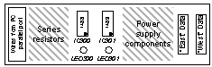
Figure 3 Suggested component layout for parallel port adapter
Because it is so simple, it may be good practice for you to construct and test the parallel port adapter circuit first. Regardless of whether you choose to wire wrap or solder your circuit, if you are not a seasoned scratch builder, starting with a small circuit is a great way to familiarise yourself with the techniques and build your confidence.
Next month, we'll explore the first of the example Linux programmes which will specifically test the parallel port interface and the ring. So even if you spend the next several months building the train controller cards, if you build the parallel port controller first, you'll be able to start playing with the software sooner rather than later.
Getting the orientation of the transistors correct
The good thing about the train controller circuit is that apart from the ICs and the voltage regulation parts, almost none of the component values are critical. This means that you should be encouraged to raid your junk boxes and to shop around for the cheapest approximate equivalents.
The transistors and relays are the two big candidates for substitution. The bad thing about substituting transistors is that often, the pin designations are not printed onto the package and there are no good standards to help you determine the pin outs by inspection alone.
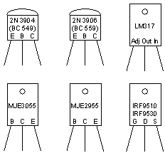
Figure 4 Likely pin outs for devices used in this project
Although I have provided a guideline of the component pin outs in Figure 4, equivalent parts from different manufacturers often have different pin outs. (The LM317 and IRF9510 are almost certainly going to be the same as above though).
It is best to be wary of the pin outs for the transistors. If a transistor does not explicitly have "EBC" designations printed on it (or "CEB" or "BEC" etc), all hobbyists would be well advised to specifically determine the pin outs before soldering them into the circuit. There are a large number of transistors in this project and if you discover a pin-out mistake after having completed construction, that’s a lot of devices to have to desolder and re-orient. If you are not thoroughly experienced in "en-mass" desoldering or if you do not have excellent desoldering tools, you should expect to irreparably damage at least some of the tracks on you matrix boards in the process. It would be better just to get the component orientations right in the first place.
If the pin outs of the transistors you have purchased are not designated, you can use a trusty old analogue multimeter, (or a higher end digital multimeter with diode testing capabilities) a couple of resistors and a battery to unequivocally determine the pin outs. The process is a little tricky but there are not that many different types of transistor in this circuit to have to test. In any case, this is an interesting and educational exercise!
To determine a transistor’s pin outs, the first task is to identify the Base and whether the transistor is NPN or PNP. Look for the transistor’s property that the both the Base – Emitter and the Base – Collector junctions will appear to behave like a simple diode.
Firstly with the analogue multimeter switched to the "x1 Ohm" scale (or digital multimeter switched to diode mode), systematically measure the "resistance" between each pair of transistor pins using both possible polarities as shown in Figure 5. Some combinations will appear to be "open" and some will appear to be low resistance – exactly the characteristics of a couple of diodes.
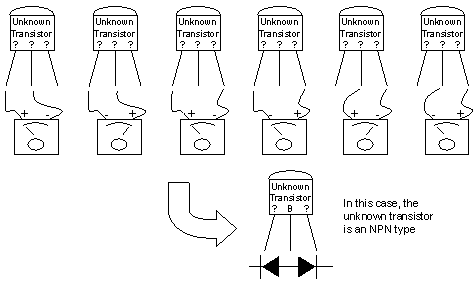
Figure 5 Six measurements to help identify a transistor’s type
After studying the results, you will notice that one of the transistor’s legs is "different" because when one particular multimeter probe is connected to it, both other transistor pins appear "open" and when the other multimeter probe is connected to it, both other transistor pins appear to be connected by a low resistance. This particular pin must therefore be the Base.
If you connected the Base to the positive probe of the multimeter in order to get a current to flow to either of the other two legs (this is the example shown in the diagram), the transistor is an NPN, otherwise it is a PNP. Caution: the positive probe of your multimeter is not necessarily the red one or the one marked +!!! You need to check the voltage polarity of the Ohm function on your particular multimeter using another Voltmeter!
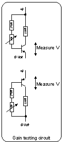
Figure 6 Identifying the Emitter and Collector on an unknown transistor
Once you have determined whether an unknown transistor is NPN or PNP and identified which of its three pins is the Base, a simple gain test circuit is required (Figure 6) to identify the Collector and Emitter pins. Transistors will usually work with their Emitter and Collectors connected back to front, but the gain and performance will be much lower when the orientation is wrong. So by comparing the gain of the two possible orientations, you can finally determine the right orientation.
At this stage, either of the remaining two unknown pins on the transistor could be the Emitter. So the transistor will need to be tested one way and then the other – the first time assuming one pin is the Emitter and the second, assuming that the other is the Emitter. There are also two test configurations shown in this diagram: one for NPN and the other for PNP. Choose the right one for the type of your unknown transistor.
With the transistor connected in one of the two possible orientations, adjust the pot until the Emitter-Collector voltage measures around half of the supply voltage. That is, if the supply voltage is 9V, adjust the pot until the Emitter-Collector voltage reads about 4.5 V. Then without changing the pot setting, swap the transistor's orientation to the other of the two possibilities and remeasure the Emitter-Collector voltage. If the second voltage reading is LOWER, the second orientation is the correct one. If the second voltage reading is HIGHER, the first orientation was the correct one.
Construction of the train controller circuit
Having obtained all your components and used them to plan your actual layout, it is time to commence wiring.
If you are new to scratch building circuits with lots of ICs, I would suggest that you take a fine tipped permanent marker (e.g. 0.8 mm) and mark the outline of each area (such as the individual block detectors) and major components (such as each DIL IC) on the solder side of the matrix board. At the same time, mark the IC number and the location of pin 1 very clearly. If you are not used to looking at a circuit from the reverse side, it is very easy to forget that the pins are numbered *clockwise* when viewed from underneath the circuit! Your scribing is going to quickly become obscured by wire and so you should not be afraid to write in large letters and numbers.
If you plan to build two or more train controller cards, then it is best if you can plan to assemble them together, component by component. The advantage of scratch building two or more cards at the same time is that they will tend to end up identical. As you progress through the construction, you are more likely to realise and correct wiring errors as you go. Then, when construction is complete and when it comes to debugging, you only have to discover the wiring bugs once and then correct them in all cards.
When building a circuit containing significant replication, you should also consider building the replicated sections first. In the case of the train controller circuit, the repetitive part of the circuit is the block detection and relays section.
There are two advantages to building the repetitive parts of a circuit first: after the first instance or two, it becomes easy to quickly add further replications without duplicating your thought processes for each. Secondly, if you discover that you have misplanned the area you allowed, you can correct your mistake when there is still plenty of room left on the blank matrix card – correcting layout misjudgements when the remainder of the card is already full of components could be more difficult.
Once the repetitive parts of the circuit are assembled, I would recommend placing all of the IC sockets onto the card and soldering them into place. In the case of wire wrap sockets, you need only solder the two power supply pins of each device. This is also a good time to solder power supply bypass capacitors between the power supply pins of each IC socket because it will become more and more difficult to add discrete parts when there are mazes of wire getting in the way.
When adding the components which require a heat sink, always make sure that you leave sufficient space around each part so that the heat sink of one component does not foul with the heat sink or body of an adjacent part. The easiest way of ensuring this is to clip the heat sink onto the transistor *before* inserting it into the matrix board so that you discover snags *before* you solder and wire the component.
Finally, remember that it is best to mount the secondary point motor driver components (transistor and resistors) adjacent to each point motor solenoid rather than centralised on your train controller card. Because the points supply power line needs to be bussed around underneath the layout to power each of these secondary point motor drivers, it is also wise to mount C16, the 2,500-10,000 uF monster capacitor, somewhere on your layout baseboard as shown in Figure 7. As point motors draw peak currents of many Amp, you should aim to minimise the I*R voltage loss by placing this capacitor as close as possible to the point motor solenoids rather than closer to the train controller cards.
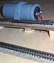
Figure 7 It is probably best to mount capacitor C16 somewhere on your baseboard rather than on the controller card itself
Whilst on the subject of the point motors, take a moment to plan your wire gauges. Between the train controller card and C16, current will be regulated to a peak of around 600 mA. You should plan to use wire which is a little heavier than standard hook-up wire for such a current. But specifically for the wiring between the capacitor and each of the point motor solenoids, the peak current could be closer to around 10 Amp and it is imperative that you choose appropriate wire for these connections (1 mm sq. or thicker if possible) and keep the length from capacitor to point coil as small as practical (shorter than 1 metre if possible).
This brings us to the end of the fifth article in the series and it was at about this stage in the building of my train set that I started to become seriously focused on it. But I can't stress firmly enough the importance of taking the time to plan and carefully construct the circuit rather than rushing in with the enthusiasm and intention of finishing it as quickly as possible. Even the most experienced constructor is unlikely to be able to finish this part of the project in fewer than half a dozen sittings, so set yourself realistic goals each time you sit down and pull out your soldering iron.
Next month, I'll take you step by step through the testing of the circuit so that by the time it comes to obtaining and compiling the example control software, you'll know that your hardware is working and the bugs could only be in the software!
Stefan Keller-Tuberg BE (Hons) MEM
Stefan Keller-Tuberg is a professional engineer with an honours degree in Electrical Engineering from the University of New South Wales and a masters degree in Engineering Management from the University of Technology, Sydney. He and his family are presently living in the United States where Stefan works in the telecommunications industry planning service architectures and product evolutions for high speed xDSL and Optical Internet access products. They are enjoying life in the USA but are looking forward to their return to Australia some time in the coming year.
Copyright 2001. Stefan Keller-Tuberg.